Ahead-looking: Researchers on the College of Massachusetts Amherst have developed a laser-based method to align 3D semiconductor chips, probably overcoming a longstanding problem in chip manufacturing. The tactic employs concentric metalenses to generate holograms that reveal misalignment between chip layers at a a lot smaller scale than beforehand potential.
Semiconductor chips have historically been manufactured in two dimensions. However as gadgets turn out to be extra highly effective and compact, the business is more and more turning to 3D chip designs, which contain stacking a number of 2D layers. This strategy introduces vital technical challenges – most notably, the necessity to align every layer with excessive precision. Even slight misalignment can compromise chip efficiency.
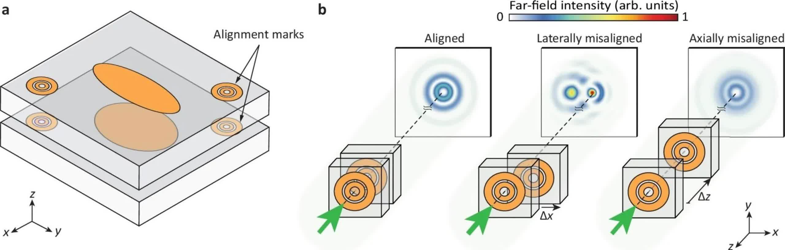
The normal strategy for aligning two layers is to look with a microscope for marks, reminiscent of corners or crosshairs, on the 2 layers and to attempt to overlap them, mentioned Amir Arbabi, affiliate professor {of electrical} and laptop engineering at UMass Amherst and senior writer of the research.
Nevertheless, this microscope-based course of is restricted by the bodily hole between layers and the necessity to refocus, which may really trigger the chips to shift and misalign additional. The microscope can’t see each crosshairs in focus directly as a result of the hole between the layers is tons of of microns. The movement required to refocus between layers can result in chip displacement, defined Maryam Ghahremani, the research’s lead writer.
Microscopes are additionally constrained by the diffraction restrict, which restricts the smallest resolvable options to about 200 nanometers.
The brand new technique developed at UMass Amherst bypasses these constraints. By embedding alignment marks manufactured from concentric metalenses onto every chip and shining a laser by means of them, the researchers generate two interfering holograms. The ensuing interference sample supplies a direct visible cue concerning the chips’ alignment ,together with each the path and magnitude of any misalignment.
“This interference picture reveals if the chips are aligned or not, in addition to the path and the quantity of their misalignment,” Ghahremani mentioned.
The system’s precision exceeded preliminary expectations. Whereas the group initially aimed for 100-nanometer accuracy, the tactic was in a position to detect misalignments as small as 0.017 nanometers alongside the horizontal axis and 0.134 nanometers alongside the vertical axis. “Contemplate you’ve got two objects. By trying on the gentle that goes by means of them, we will see if one moved by the scale of an atom with respect to the opposite one,” Arbabi mentioned.
This degree of precision might have main implications for the semiconductor business, the place alignment errors stay a persistent and dear problem. Decreasing the technical and monetary limitations to ultra-precise chip alignment might make superior manufacturing extra accessible to smaller corporations and startups.
The researchers additionally counsel that the method may very well be tailored for compact, low-cost sensors. “Many bodily portions that you simply wish to detect may be translated to displacements, and the one factor you want is an easy laser and a digicam,” Arbabi mentioned. Functions might embrace stress sensors, vibration detectors, and different gadgets that monitor motion or environmental modifications.


